XC6VLX130T-2FF1156C
- Part Number: XC6VLX130T-2FF1156C
- Categories:
- Manufacturer: Xilinx
- MOQ: 1PCS
- In Stock: 17083
- Datasheet:
- Description: IC FPGA 600 I/O 1156FCBGA
- Payment method: Paypal/Wire transfer/Visa
- Delivery Method: UPS/DHL/FEDEX/EMS
- 1 Pcs$33.711
- 10 Pcs$32.105
- 100 Pcs$30.576
- 1000 Pcs$29.977
- 10000 Pcs$29.977
| Manufacturer | Xilinx |
| Mounting Type | Surface Mount |
| Number of I/O | 600 |
| Package / Case | 1156-BBGA, FCBGA |
| Product Status | Active |
| Total RAM Bits | 9732096 |
| Number of Gates | - |
| Voltage - Supply | 0.95V ~ 1.05V |
| Number of LABs/CLBs | 10000 |
| Operating Temperature | 0°C ~ 85°C (TJ) |
| Supplier Device Package | 1156-FCBGA (35x35) |
| Number of Logic Elements/Cells | 128000 |
XC6VLX130T-2FF1156C FPGAs Overview
Description:
Virtex®-6 FPGAs are the programmable silicon foundation for Targeted Design Platforms that deliver integrated software and hardware components to enable designers to focus on innovation as soon as their development cycle begins. Using the third-generation ASMBL™ (Advanced Silicon Modular Block) column-based architecture, the Virtex-6 family contains multiple distinct sub-families. This overview covers the devices in the LXT, SXT, and HXT sub-families. Each sub-family contains a different ratio of features to most efficiently address the needs of a wide variety of advanced logic designs. In addition to the high-performance logic fabric, Virtex-6 FPGAs contain many builtin system-level blocks. These features allow logic designers to build the highest levels of performance and functionality into their FPGAbased systems. Built on a 40 nm state-of-the-art copper process technology, Virtex-6 FPGAs are a programmable alternative to custom ASIC technology. Virtex-6 FPGAs offer the best solution for addressing the needs of high-performance logic designers, high-performance DSP designers, and high-performance embedded systems designers with unprecedented logic, DSP, connectivity, and soft microprocessor capabilities.
Summary of Virtex-6 FPGA
Features:
• Three sub-families:
• Virtex-6 LXT FPGAs: High-performance logic with advanced serial connectivity
• Virtex-6 SXT FPGAs: Highest signal processing capability with advanced serial connectivity
• Virtex-6 HXT FPGAs: Highest bandwidth serial connectivity
• Compatibility across sub-families
• LXT and SXT devices are footprint compatible in the same package
• Advanced, high-performance FPGA Logic
• Real 6-input look-up table (LUT) technology
• Dual LUT5 (5-input LUT) option
• LUT/dual flip-flop pair for applications requiring rich register mix
• Improved routing efficiency
• 64-bit (or two 32-bit) distributed LUT RAM option per 6-input LUT
• SRL32/dual SRL16 with registered outputs option
• Powerful mixed-mode clock managers (MMCM)
• MMCM blocks provide zero-delay buffering, frequency synthesis, clock-phase shifting, inputjitter filtering, and phase-matched clock division
• 36-Kb block RAM/FIFOs
• Dual-port RAM blocks
• Programmable - Dual-port widths up to 36 bits - Simple dual-port widths up to 72 bits
• Enhanced programmable FIFO logic
• Built-in optional error-correction circuitry
• Optionally use each block as two independent 18 Kb blocks
• High-performance parallel SelectIO™ technology
• 1.2 to 2.5V I/O operation
• Source-synchronous interfacing using ChipSync™ technology
• Digitally controlled impedance (DCI) active termination
• Flexible fine-grained I/O banking
• High-speed memory interface support with integrated write-leveling capability
• Advanced DSP48E1 slices
• 25 x 18, two's complement multiplier/accumulator
• Optional pipelining
• New optional pre-adder to assist filtering applications
• Optional bitwise logic functionality
• Dedicated cascade connections
• Flexible configuration options
• SPI and Parallel Flash interface
• Multi-bitstream support with dedicated fallback reconfiguration logic
• Automatic bus width detection
• System Monitor capability on all devices
• On-chip/off-chip thermal and supply voltage monitoring
• JTAG access to all monitored quantities
• Integrated interface blocks for PCI Express® designs
• Compliant to the PCI Express Base Specification 2.0
• Gen1 (2.5 Gb/s) and Gen2 (5 Gb/s) support with GTX transceivers
• Endpoint and Root Port capable
• x1, x2, x4, or x8 lane support per block
• GTX transceivers: up to 6.6 Gb/s
• Data rates below 480 Mb/s supported by oversampling in FPGA logic.
• GTH transceivers: 2.488 Gb/s to beyond 11 Gb/s
• Integrated 10/100/1000 Mb/s Ethernet MAC block
• Supports 1000BASE-X PCS/PMA and SGMII using GTX transceivers
• Supports MII, GMII, and RGMII using SelectIO technology resources
• 2500Mb/s support available
• 40 nm copper CMOS process technology
• 1.0V core voltage (-1, -2, -3 speed grades only)
• Lower-power 0.9V core voltage option (-1L speed grade only)
• High signal-integrity flip-chip packaging available in standard or Pb-free package options
Features
Three sub-families:
Virtex-6 LXT FPGAs: High-performance logic with advanced serial connectivity
Virtex-6 SXT FPGAs: Highest signal processing capability with advanced serial connectivity
Virtex-6 HXT FPGAs: Highest bandwidth serial connectivity
Compatibility across sub-families
LXT and SXT devices are footprint compatible in the same package
Advanced, high-performance FPGA Logic
Powerful mixed-mode clock managers (MMCM)
MMCM blocks provide zero-delay buffering, frequency synthesis, clock-phase shifting, inputjitter filtering, and phase-matched clock division
36-Kb block RAM/FIFOs
High-performance parallel SelectIO technology
1.2 to 2.5V I/O operation
Source-synchronous interfacing using ChipSync technology
Digitally controlled impedance (DCI) active termination
Flexible fine-grained I/O banking
High-speed memory interface support with integrated write-leveling capability
Advanced DSP48E1 slices
25 x 18, two`s complement multiplier/accumulator
Optional pipelining
New optional pre-adder to assist filtering applications
Optional bitwise logic functionality
Dedicated cascade connections
Flexible configuration options
GTX transceivers: up to 6.6 Gb/s
Data rates below 480 Mb/s supported by oversampling in FPGA logic.
GTH transceivers: 2.488 Gb/s to beyond 11 Gb/s
Integrated 10/100/1000 Mb/s Ethernet MAC block
Supports 1000BASE-X PCS/PMA and SGMII using GTX transceivers
Supports MII, GMII, and RGMII using SelectIO technology resources
2500Mb/s support available
40 nm copper CMOS process technology
1.0V core voltage (-1, -2, -3 speed grades only)
Lower-power 0.9V core voltage option (-1L speed grade only)
High signal-integrity flip-chip packaging available in standard or Pb-free package options
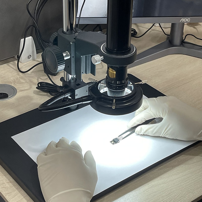
 step1: Inspect Products
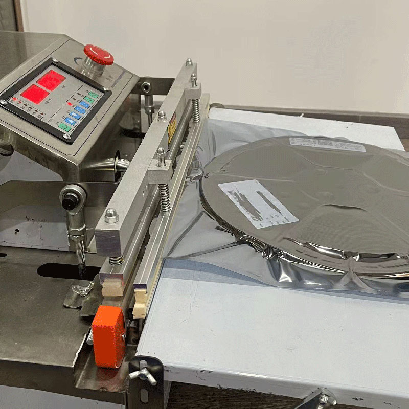
 step2: Vacuum Packaging
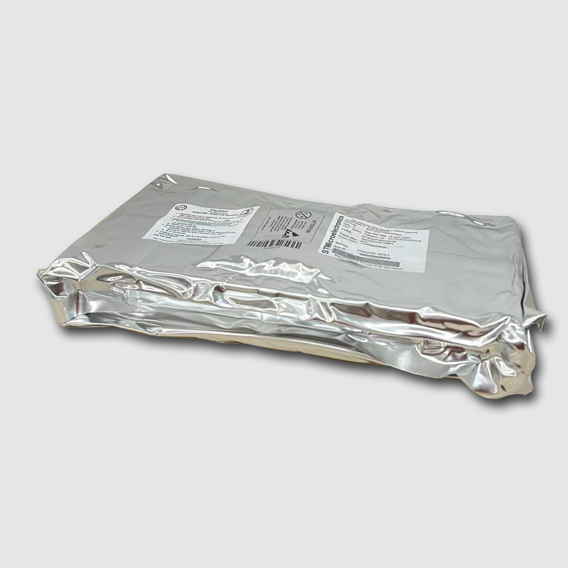
 step3: Anti-Static Bag
 step4: Individual Packing
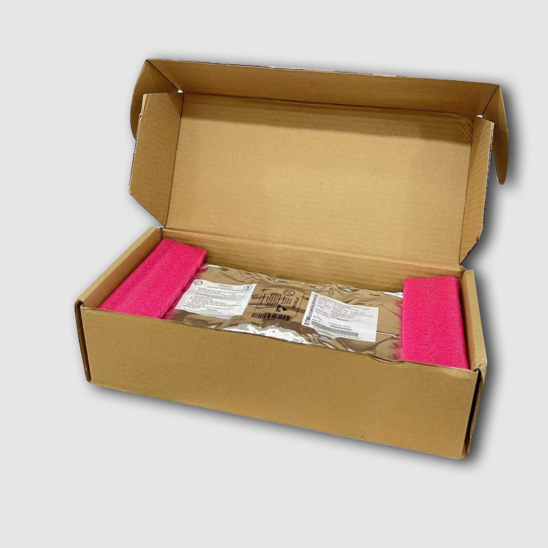
 step5: Packing Box
 step6:Shipping Tag

- Before shipping, we will inspect the parts to ensure it in good condition and check that the parts are brand-new and original with the datasheet. And then, all the products will be packed in an anti-static bag.
- After ensuring that there are no issues with any of the goods after packing, we will wrap them carefully and send them by international express. It demonstrates exceptional seal integrity, outstanding tear and puncture resistance, and both.

Xilinx is a leading provider of programmable logic devices and associated technologies. As a top producer of programmable FPGAs, SoCs, MPSoCs, and 3D ICs, Xilinx has expanded quickly. Software defined and hardware optimized applications are supported by Xilinx, advancing the fields of cloud computing, SDN/NFV, video/vision, industrial IoT, and 5G wireless.
One of Xilinx's key innovations is the development of the Xilinx Vivado Design Suite, a comprehensive software toolchain used for designing and programming their FPGAs and SoCs. This suite provides developers with the necessary tools to create, simulate, and implement their designs on Xilinx devices.
In October 2020, Xilinx was acquired by Advanced Micro Devices (AMD), a major player in the semiconductor industry. This acquisition has enabled AMD to enhance its product portfolio and expand its offerings into the rapidly growing FPGA market.
- Ultra-low power consumption of STM32U575/585 microcontrollers(MCU)
- The STM32U575/585 microcontrollers (MCU) are based on the high-performance Arm 32-bit Cortex‑M33CPU with Arm TrustZone and FPU.
- TI(Texas Instruments)Advanced Ultrasonic Lens Cleaning Chipset Enables Self-Cleaning Cameras and Sensors
- Computer vision and advanced imaging have enabled many revolutionary technologies, one of the most important being Advanced Driver Assistance Systems (ADAS) and autonomous vehicles.
- The Best Guide to Transistor
- The transistor is electronic equipment. It is made through a p and n-type semiconductor. When a semiconductor is placed in the center between the same type of semiconductors the arrangement is called transistors.
- Electronic Component Symbols: Resistor, Capacitor, Transformers and Connectors
- Electronic components are components of electronic components and small machines and instruments. They are often composed of several parts and can be used in similar products.
- Basic Information about Temperature Sensor
- A temperature transducer is a sensor that can sense temperature and convert it into a usable output signal. The temperature sensor is the core part of the temperature measuring instrument, and there are many varieties. After entering the 21st century, temperature sensors are rapidly developing towards high-tech directions such as high precision, multi-function, bus standardization, high reliability and safety, development of virtual sensors and network sensors, and development of single-chip temperature measurement systems. The bus technology of the temperature sensor has also been standardized, and it can be used as a slave to communicate with the host through a dedicated bus interface. According to the measurement method, it can be divided into two categories: a contact type and a non-contact type. According to the characteristics of sensor materials and electronic components, it can be divided into two types: thermal resistance and thermocouple. Main Category The detection part of the contact temperature sensor is in good contact with the measured object, also known as a thermometer. The thermometer achieves heat balance through conduction or convection so that the indication value of the thermometer can directly represent the temperature of the measured object. Generally, the measurement accuracy is high. Within a certain temperature range, the thermometer can also measure the temperature distribution inside the object. However, large measurement errors will occur for moving bodies, small targets, or objects with small heat capacity. Commonly used thermometers include bimetallic thermometers, liquid-in-glass thermometers, pressure thermometers, resistance thermometers, thermistors, and thermocouples. They are widely used in industry, agriculture, commerce, and other sectors. People also often use these thermometers in daily life. With the wide application of cryogenic technology in national defense engineering, space technology, metallurgy, electronics, food, medicine, petrochemical, and other departments and the research of superconducting technology, cryogenic thermometers for measuring temperatures below 120K have been developed, such as cryogenic gas thermometers, steam Pressure thermometers, acoustic thermometers, paramagnetic salt thermometers, quantum thermometers, low-temperature thermal resistance, and low-temperature thermocouples, etc. Cryogenic thermometers require small temperature sensing elements, high accuracy, good reproducibility, and stability. The carburized glass thermal resistance made of porous high silica glass carburized and sintered is a kind of temperature sensing element of the low-temperature thermometer, which can be used to measure the temperature in the range of 1.6 ~ 300K. Its sensitive components are not in contact with the measured object, also known as a non-contact temperature measuring instrument. This instrument can be used to measure the surface temperature of moving objects, small targets, and objects with small heat capacity or rapid temperature changes (transient), and can also be used to measure the temperature distribution of the temperature field. The most commonly used non-contact thermometers are based on the fundamental law of black body radiation and are called radiation thermometers. Radiation thermometry methods include the brightness method (see optical pyrometer), radiation method (see radiation pyrometer), and colorimetric method (see colorimetric thermometer). All kinds of radiation temperature measurement methods can only measure the corresponding photometric temperature, radiation temperature, or colorimetric temperature. Only the temperature measured for a black body (an object that absorbs all radiation and does not reflect light) is the true temperature. If you want to measure the real temperature of the object, you must correct the surface emissivity of the material. However, the surface emissivity of materials depends not only on temperature and wavelength, but also on surface state, coating film, and microstructure, so it is difficult to measure accurately. In automatic production, it is often necessary to use radiation thermometry to measure or control the surface temperature of certain objects, such as the steel strip rolling temperature, roll temperature, forging temperature in metallurgy, and the temperature of various molten metals in smelting furnaces or crucibles. In these specific cases, the measurement of the emissivity of an object's surface is quite difficult. For automatic measurement and control of solid surface temperature, an additional reflector can be used to form a black body cavity together with the measured surface. The effect of additional radiation can increase the effective radiation and effective emissivity of the measured surface. Use the effective emissivity coefficient to correct the measured temperature through the instrument, and finally get the real temperature of the measured surface. The most typical additional mirror is hemispherical. The diffuse radiation on the measured surface near the center of the sphere can be reflected on the surface by the hemispherical mirror to form additional radiation, thereby increasing the effective emissivity coefficient. In the formula, ε is the surface emissivity of the material, and ρ is the reflectivity of the mirror. As for the radiation measurement of the real temperature of the gas and liquid medium, the method of inserting the heat-resistant material tube to a certain depth to form a black body cavity can be used. The effective emission coefficient of the cylinder cavity after reaching thermal equilibrium with the medium is obtained by calculation. In automatic measurement and control, this value can be used to correct the measured cavity bottom temperature (ie medium temperature) to obtain the real temperature of the medium. Advantages of non-contact temperature measurement: the upper limit of measurement is not limited by the temperature resistance of the temperature sensing element, so there is no limit to the maximum measurable temperature in principle. For high temperatures above 1800°C, non-contact temperature measurement methods are mainly used. With the development of infrared technology, radiation temperature measurement has gradually expanded from visible light to infrared and has been used below 700°C to room temperature with high resolution. Working principle Metals undergo a corresponding extension when the ambient temperature changes, so the sensor can signal this response in different ways. Bimetal Sensor A bimetal sheet is composed of two pieces of metal with different expansion coefficients attached. As the temperature changes, material A expands more than the other metal, causing the metal sheet to bend. The curvature of the bend can be converted into an output signal. Bimetal Rod and Tube Sensors As the temperature increases, the length of the metal tube (material A) increases, while the length of the non-expanding steel rod (metal B) does not increase so that the linear expansion of the metal tube can be transmitted due to the change of position. In turn, this linear expansion can be translated into an output signal. Deformation Curve Design Sensors for Liquids and Gases When the temperature changes, liquids, and gases will also produce corresponding changes in volume. Various types of structures can convert this change in expansion into a change in position, thus producing a position change output (potentiometer, sense bias, baffle, etc.). Resistance sensing As the temperature of the metal changes, its resistance value also changes. For different metals, every time the temperature changes by one degree, the resistance value changes differently, and the resistance value can be directly used as an output signal. There are two types of changes in resistance positive temperature coefficient Increased temperature = increased resistance A decrease in temperature = a decrease in resistance negative temperature coefficient Increased temperature = decreased resistance Decrease in temperature = increase in resistance Thermocouple Sensing A thermocouple consists of two metal wires of different materials welded together at the ends. Then measure the ambient temperature of the non-heating part, and the temperature of the heating point can be accurately known. Since it must have two conductors of different materials, it is called a thermocouple. Thermocouples made of different materials are used in different temperature ranges, and their sensitivities also vary. The sensitivity of the thermocouple refers to the change in the output potential difference when the temperature of the heating point changes by 1 °C. For most thermocouples supported by metallic materials, this value is between 5 and 40 microvolts/°C. Since the sensitivity of the thermocouple temperature sensor has nothing to do with the thickness of the material, it can also be made into a temperature sensor with very thin materials. Also due to the good ductility of the metal material used to make thermocouples, this tiny temperature-measuring element has a very high response speed and can measure rapidly changing processes. Selection method If you want to make reliable temperature measurements, you first need to choose the correct temperature instrument, that is, the temperature sensor. Among them, thermocouples, thermistors, platinum resistance thermometers (RTDs), and temperature ICs are the most commonly used temperature sensors in testing. The following is an introduction to the characteristics of the thermocouple and thermistor temperature instruments. thermocouple Thermocouples are the most commonly used temperature sensors in temperature measurement. Its main advantages are a wide temperature range and adaptability to various atmospheric environments, and it is strong, low in price, does not require a power supply, and is the cheapest. A thermocouple consists of two wires of dissimilar metals (metal A and metal B) connected at one end. When one end of the thermocouple is heated, there is a potential difference in the thermocouple circuit. The temperature can be calculated from the measured potential difference. However, there is a nonlinear relationship between voltage and temperature. Since the temperature is a nonlinear relationship between voltage and temperature, it is necessary to make a second measurement for the reference temperature (Tref), and use the test equipment software or hardware to process the voltage-temperature conversion inside the instrument, to Finally the thermocouple temperature (Tx), is obtained. Both Agilent34970A and 34980A data collectors have built-in measurement computing capabilities. In short, thermocouples are the simplest and most versatile temperature sensors, but thermocouples are not suitable for high-precision measurements and applications. Thermistors are made of semiconductor materials, and most of them have a negative temperature coefficient, that is, the resistance value decreases with the increase in temperature. Temperature changes will cause large resistance changes, so it is the most sensitive temperature sensor. However, the linearity of the thermistor is extremely poor and has a lot to do with the production process. Manufacturers do not give standardized thermistor curves. Thermistors are very small and respond quickly to changes in temperature. But the thermistor requires a current source, and its small size makes it extremely sensitive to self-heating errors. The thermistor measures absolute temperature on two lines and has better accuracy, but it is more expensive than a thermocouple, and its measurable temperature range is also smaller than that of a thermocouple. A commonly used thermistor has a resistance of 5kΩ at 25°C, and every 1°C temperature change causes a resistance change of 200Ω. Note that the 10Ω lead resistance causes only a negligible 0.05°C error. It is ideal for current control applications requiring fast and sensitive temperature measurements. The small size is advantageous for applications with space requirements, but care must be taken to prevent self-heating errors. Thermistors also have their measurement tricks. The advantage of the thermistor's small size is that it stabilizes quickly without causing a thermal load. However, it is also very weak, and a high current will cause self-heating. Since the thermistor is a resistive device, any current source will generate heat from power across it. Power is equal to the product of the square of the current and the resistance. So use a small current source. Permanent damage will result if the thermistor is exposed to high heat.
- Do you Know BD140 PNP Transistor: Pinout, Datasheet, Features and Applications
- The BD140 is a medium power bipolar junction PNP transistor that is mainly used for audio amplifiers and drivers utilizing complementary or quasi-complementary circuits. It is made up of silicon and comes in the TO-126 package.


