What is XC7A100T-2FG484I?
Introduction
The Xilinx Artix®-7 family of FPGAs offers the best performance-per-watt fabric, DSP processing, transceiver line rates, and AMS integration in an FPGA that is tailored for affordability. The series provides the best value for a range of price- and power-sensitive applications, such as software-defined radio, machine vision cameras, and low-end wireless backhaul, thanks to its MicroBlazeTM soft processor and 1,066Mb/s DDR3 compatibility. It is designed with low power consumption, high DSP, and logic throughput applications in mind. Up to 215K logic cells, an x4 Gen2 PCIe interface, 500 I/O pins, 13Mb BRAM, 740 DSP slices, 929 GMAC/s, 16 transceivers, 6.6Gb/s transceiver speed, and 211Gb/s serial bandwidth are among its capabilities. A wide range of configuration options are supported by the Artix®-7 FPGA, such as commodity memory support, 256-bit AES encryption with HMAC/SHA-256 authentication, and integrated SEU detection and correction. It satisfies the requirements of SWaP-C—size, weight, power, and cost-sensitive industries like communications and aviation.
Table of Content
What is XC7A100T-2FGG484I?
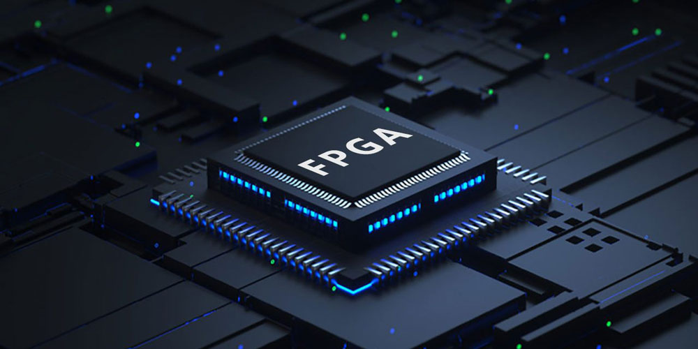
An integrated circuit with 285 I/O, 7925 LABs/CLBs, and 101440 logic elements/cells is the Xilinx Inc. XC7A100T-2FGG484I. It comes in a 484-FBGA (23x23) packaging and has a total of 48676640 RAM bits. The XC7A100T-2FGG484I has a supply voltage range of 0.95V to 1.05V and operates between -40°C and 100°C (TJ). This integrated circuit has a high fake danger and is widely used in the market. There is a balance between supply and demand.

Figure1- XC7A100T-2FGG484I
XC7A100T-2FGG484I CAD Model

Figure2-Symbol

Figure3-Footprint

Figure4-3d model
XC7A100T-2FGG484I Features
- Sophisticated FPGA logic with distributed memory capabilities, based on actual 6-input lookup table (LUT) technology.
- 36 Kb dual-port block RAM with built-in FIFO logic for on-chip data buffering.
- SelectIOTM technology offers high performance and supports DDR3 interfaces up to 1,866 Mb/s.
- High-speed serial connectivity with integrated multi-gigabit transceivers that can operate at up to 600 Mb/s and 6.6 Gb/s at maximum rates, as well as a unique low-power mode that is designed with chip-to-chip interfaces in mind.
- A user-configurable analog interface (XADC), incorporating dual 12-bit 1MSPS analog-to-digital converters with on-chip thermal and supply sensors.
- An XADC, or user-configurable analog interface, has two 12-bit 1MSPS analog-to-digital converters along with on-chip supply and temperature sensors.
- DSP slices with 25 x 18 multiplier, 48-bit accumulator, and pre-adder for high-performance filtering, including optimized symmetric coefficient filtering.
- Strong clock management tiles (CMT) that combine mixed-mode clock manager (MMCM) and phase-locked loop (PLL) blocks for minimal jitter and maximum precision.
- Integrated block supporting up to x8 Gen3 Root Port and Endpoint designs using PCI Express® (PCIe).
- several configuration options, such as integrated SEU detection and correction, 256-bit AES encryption with HMAC/SHA-256 authentication, and compatibility for commodity memory.
- Flipchip packaging that is low-cost, wire-bond, lidless, and has strong signal integrity allows for simple migration amongst family members within the same package. All packages have Pb-free options and some products with Pb option available.
- High performance and low power consumption were the design goals, with a 1.0V core voltage process, HKMG, HPL process, 28 nm, and a 0.9V core voltage option for even lower power.
XC7A100T-2FGG484I Specification
|
Categories |
Integrated Circuits |
|
Manufacturer |
Xilinx Inc. |
|
Status |
Active |
|
Number of LABs/CLBs |
7925 |
|
Number of Logic Elements/Cells |
101440 |
|
Total RAM Bits |
4976640 |
|
Number of I/O |
285 |
|
Supply Voltage - Operating |
0.95 V to 1.05 V |
|
Mounting |
SMD (SMT) |
|
Temperature Range - Operating |
-40°C to 100°C (TJ) |
|
Case / Package |
484-FBGA (23x23) |
|
Win Source Part Number |
084574-XC7A100T-2FGG484I |
|
Is this a commonly used part? |
Yes |
|
Popularity |
High |
|
Fake Threat In the Open Market |
43 pct. |
|
Supply and Demand Status |
Balance |
|
Family Name |
XC7A100T |
|
Introduction Date |
June 21, 2010 |
|
ECCN |
3A991.d |
|
Country of Origin |
Republic of Korea, Taiwan |
|
Estimated EOL Date |
2022 |
|
Alternative Parts |
M1A3P1000L-1FGG484Y; A3P1000L-FGG484YI; M1A3P1000L-FGG484Y; |
XC7A100T-2FGG484I Applications
The versatility of the XC7A100T-2FGG484I makes it suitable for a wide range of applications:
Communications: Its high-speed transceivers and DSP slices make it ideal for implementing complex communication protocols and signal-processing tasks.
Embedded Systems: With ample logic cells and I/O pins, this FPGA can serve as the core of sophisticated embedded systems, handling everything from control logic to data processing.
Medical Devices: The combination of low power consumption and high performance makes it suitable for portable medical devices requiring reliable and precise operation.
Industrial Automation: The robust performance and flexibility of this FPGA make it perfect for controlling machinery, processing sensor data, and other automation tasks.
Consumer Electronics: The FPGA's capabilities can enhance the performance and features of consumer electronics, from high-end audio processing to advanced camera systems.
XC7A100T-2FGG484I Benefits
Flexibility: The primary advantage of FPGAs is their programmability. The XC7A100T-2FGG484I can be reconfigured to perform different tasks, offering significant flexibility over fixed-function ASICs.
Performance: With dedicated DSP slices and efficient logic cells, this FPGA can perform complex computations at high speeds, making it suitable for real-time applications.
Power Efficiency: The 28nm process technology ensures low power consumption, a critical factor for many modern electronic devices.
Scalability: As part of the Xilinx 7 Series, this FPGA is compatible with other devices in the family, allowing for scalable solutions across different performance and cost requirements.
XC7A100T-2FGG484I Datasheet
XC7A100T-2FGG484I manufacturer
The top supplier of comprehensive programmable logic solutions worldwide is Xilinx. A vast array of cutting-edge integrated circuits, software development tools, and IP (intellectual property) cores as preset system-level characteristics are developed, produced, and marketed by Xilinx. Customers program specific logic processes using IP verification devices and automation software solutions from Xilinx and its partners.
Founded in 1984, Xilinx pioneered the innovative technology of Field Programmable Logic Array (FPGA) and first introduced commercial products in 1985. At the moment, Xilinx meets more than half of the world's demand for FPGA products.
 A Comprehensive Guide to Grasping FPGA Structure6/20/2024 381
FPGA (Field-Programmable Gate Array) is an integrated circuit, a type of programmable chip, that allows engineers to program custom digital logic. It can change its hardware logic based on the program, with the primary purpose of enabling engineers to redesign and reconfigure their chips faster and cheaper, whenever they want. However, nothing in the world is ideal, and FPGA chips also have limitations!
Read More > The EU to Impose Tariffs on Electric Vehicle Imports from China in Early July6/17/2024 265
The EU to Impose Tariffs on Electric Vehicle Imports from China in Early July
Read More > Analog cycle inventory hits bottom, AI drives flash memory demand to continue6/4/2024 397
Analog cycle inventory hits bottom, AI drives flash memory demand to continue
Read More > Micron Plans to Build a Factory in Japan, NAND Flash Prices May Remain High5/31/2024 477
Micron Plans to Build a Factory in Japan, NAND Flash Prices May Remain High
Read More > HBM production capacity is squeezing out-DRAM memory may be in short supply in the second half of the year5/28/2024 326
HBM production capacity is squeezing out, DRAM memory may be in short supply in the second half of the year
Read More >
Hot News
- Diode Overview: Application in Automotive Alternator Rectifiers
- Voltage-Controlled Oscillator: Principle, Type Selection, and Application
- Ultra-low power consumption of STM32U575/585 microcontrollers(MCU)
- Electronic Component Symbols: Resistor, Capacitor, Transformers and Connectors
- The Best Guide to Transistor
- Basic Information about Temperature Sensor


