A Comprehensive Guide to Grasping FPGA Structure
What is FPGA?
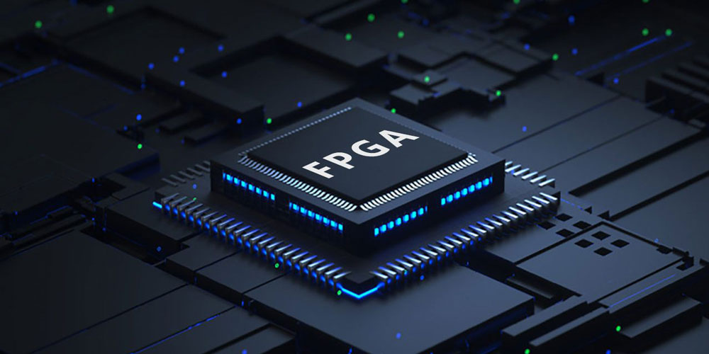
FPGA (Field-Programmable Gate Array) is an integrated circuit, a type of programmable chip, that allows engineers to program custom digital logic. It can change its hardware logic based on the program, with the primary purpose of enabling engineers to redesign and reconfigure their chips faster and cheaper, whenever they want. However, nothing in the world is ideal, and FPGA chips also have limitations!
FPGA first appeared in the 1980s, initially used to provide engineers with a general-purpose programmable logic chip. However, this required a lot of programming to perform simple functions, so engineers tried to avoid using these features. Although FPGAs in the 1980s were simple interface devices, mainly targeted at glue logic which was difficult to use for designing complex systems, they have evolved into system-level integrated circuits with their own memory blocks, microprocessors, and interfaces, allowing for the design of significant systems.
FPGA Features
Using FPGA to design ASIC (Application-Specific Integrated Circuit) circuits allows users to obtain functional chips without the need for production tape-out.
FPGA can serve as a prototype chip for other full-custom or semi-custom ASIC circuits.
FPGA has abundant internal flip-flops and I/O pins.
FPGA is one of the devices with the shortest design cycle, lowest development cost, and least risk in ASIC circuits.
FPGA uses high-speed CMOS technology, which has low power consumption and can be compatible with CMOS and TTL levels.
It enables engineers to precisely build the required hardware without using standard integrated circuits or incurring the time, cost, and risks associated with ASIC design.
Compared to microprocessors or microcontrollers, they operate in a faster, more energy-efficient, and simpler manner.
FPGA functionality can be updated like any other software code, even after the hardware has left the production site. This helps to fix bugs or add new features.

Figure2-FPGA Advantage
It can be said that FPGA chips are one of the best choices for improving system integration and reliability. FPGA is configured by a program stored in the on-chip RAM, so it requires programming the on-chip RAM during operation. Users can adopt different programming methods based on different configuration modes. When powered on, the FPGA chip reads data from the EPROM into the on-chip programming RAM, and after configuration is complete, the FPGA enters the operational state. When power is lost, the FPGA reverts to a blank state, and the internal logical connections disappear, thus allowing the FPGA to be reused repeatedly. FPGA programming does not require a dedicated FPGA programmer; a general-purpose EPROM or PROM programmer will suffice. When it is necessary to modify the FPGA functions, simply replacing the EPROM is enough. Therefore, the same FPGA chip can generate different circuit functions with different programming data. This makes the use of FPGA very flexible.
CPLD vs FPGA
CPLD (Complex Programmable Logic Device) is also a device that can be reprogrammed after manufacturing. In this sense, it is similar to FPGA. However, there are significant differences. FPGA is composed of multiple logic units, whereas CPLD consists of fewer logic units. Due to their size, CPLDs are usually cheaper and faster. However, the functionality of CPLDs is very limited; they cannot be used to build complex systems and are typically used for simple designs, such as glue logic.

Figure3-CPLD and FPGA Archiectures
Different manufacturers have different terminologies. PLD (Programmable Logic Device) is a general term for programmable logic devices. Early PLDs mostly used EEPROM technology and were based on a product term structure. FPGA was first invented by Xilinx. They typically use SRAM technology, are based on a Look-Up Table (LUT) structure, and require an external EPROM for configuration. Xilinx calls PLDs that use SRAM technology and require an external EPROM for configuration FPGA, while PLDs that use Flash technology (similar to EEPROM technology) and a product term structure are called CPLD. Altera calls its PLD products the MAX series (EEPROM technology) and FLEX/ACEX/APEX series (SRAM technology) CPLD, or Complex PLD.

Figure4-CPLD vs FPGA
FPGA Architecture
FPGA is composed of building blocks, which are like Lego bricks that can be used to construct systems. It has a basic logic building block called a Configurable Logic Block (CLB), but it can also contain larger blocks, such as PLLs (Phase-Locked Loops), interfaces, memory, and more. A single FPGA chip will have hundreds of thousands of logic units. In addition to CLBs, the chip also has Input Output Blocks (IOB) and internal interconnects.

Figure5-FPGA Architecture
We have a Look-Up Table (LUT) as the core of the FPGA logic block. Essentially, it is a RAM. After writing data into the RAM in advance, whenever an input signal is received, it acts as an address to look up the table, find the content corresponding to the address, and then output it. The output of the building block is multiplexed. One input of the multiplexer is the direct output of the LUT, used for pure combinational logic, such as NAND, NOR, XOR, or other logic gates. The other input of the multiplexer is the registered output of the LUT, which is stored and synchronized with the clock using a D-type flip-flop.
A single logic unit by itself is a simple circuit and cannot accomplish much, but when there are many logic units, we can achieve any functionality we desire. To do this, logic units are connected to an array of other logic units.

Figure6-logic units
The orange rectangles between CLB blocks are programmable switches, which can route the output of logic units anywhere. This is a very simplified diagram; in reality, there are more wires and interconnect lines than shown here.
Notice the carry-in and carry-out pins. Each adder is only one bit wide, but by using the carry-in/carry-out pins, large adders and counters can be created very quickly and efficiently. Having fast, dedicated carry chains is one of the biggest advantages of FPGA over other programmable logic devices like CPLD.
In FPGA, the clock can drive all the flip-flops, as digital design without a clock is almost unimaginable. FPGAs have very advanced clock resources, including built-in configurable PLLs (Phase-Locked Loops) and DLLs (Delay-Locked Loops). Since almost all modern digital designs require multiple clocks with different frequencies and phase delays, clock management is very important.
FPGAs also have input/output blocks for reading and outputting data. In addition to standard I/O blocks, most FPGAs have the following I/O features:
Trigger output synchronized I/O
Differential signals
Double Data Rate (DDR)
Serializer and deserializer (SERDES)
Pull-up, pull-down, and tri-state I/O
Adjustable turnaround speed, adjustable drive strength
Like built-in RAM blocks in memory, distributed RAM can vary between 100 Kb and 100 Mb. The latest generation of FPGA devices also has DSP multiplier slices, mainly used for DSP applications (digital signal processing). Most FPGAs have other built-in blocks as well.
ADC and DAC
External memory controllers, such as DRAM, DDR, DDR2.
Serial bus controller
Ethernet MAC
Dedicated FIFO [2]
High-speed transceiver
These blocks are designed as "hard blocks" on FPGA devices, rather than constructed from logic blocks and switches after the manufacturing process because they are typically required by all complex systems. Since they exist in all systems and are used very frequently, we want them to be present to save time (it makes no sense to design them from scratch using CLBs and switches each time; instead, we design them as separate configurable blocks so that designers can change their parameters). However, more importantly, we want them to have very good characteristics, work very efficiently, and occupy less space. Additionally, some analog components in these modules need to be manually designed and cannot be constructed solely through digital units.
How do I program and configure an FPGA?
To configure an FPGA, we need to program it. We can use FPGA hardware description languages such as Verilog, SystemVerilog, and VHDL for programming. These languages have some differences, which we won't go into detail about here. The workflow for defining hardware using an FPGA is as follows:

Figure7-program and configure an FPGA
"Each step requires a set of tools. Most FPGA manufacturers provide programming environments equipped with all the necessary tools."
Xilinx
Founded in 1984, Xilinx pioneered the innovative field programmable logic array (FPGA) technology and launched its first commercial product in 1985. It is the world's leading supplier of complete programmable logic solutions and is currently the number one FPGA solution provider.

Figure8-Xilinx
The product series include:
Spartan series: positioned in the low-end market, the latest device is Spartan7 using a 28nm process;
Artix series: positioned in the mid-end market between low-end Spartan and high-end Kintex, the mainstream product currently on sale is Artix-7 using a 28nm process;
Kintex series: positioned in the high-end market, including Kintex7 series using 28nm process, Kintex7 Ultrascale series using 20nm, and Kintex7 Ultrascale+ series using 16nm;
Virtex series: positioned in the high-end market, including Virtex7 series using 28nm process, Virtex7 Ultrascale series using 20nm, and Virtex7 Ultrascale+ series using 16nm;
Fully programmable SoC and MPSoC series: including Zynq-7000 and Zynq UltraScale+ MPSoC series FPGAs, embedded with ARM Cortex series CPUs;
AI Engine series: Versal ACAP, Alveo series, etc.
Intel(Altera)
The product series include:
MAXII series: essentially CPLD;
Cyclone series: positioned in the low-end market, similar to Xilinx's Spartan series and Artix series, the latest product is Cyclone10.
Stratix series: positioned in the high-end market, competing with Xilinx's Kintex and Virtex series, the latest product is Stratix10;
Arria series: SOC series FPGA, built-in ARM Cotex A9 core;
Intel Arria 10 series: FPGA that supports DDR4 memory interface, hardware designers can use Quartus II software v14.1 to achieve 666 Mbps DDR4 memory data rate in Arria 10 FPGA and SoC design;
Agilex series: Targeting high-end markets such as data centers, an FPGA product using a 10nm process, and heterogeneous 3D system-level packaging (SiP) technology.
Microchip(Microsemi)
Microsemi acquired Actel and focused on the US military and aviation fields. Its products are mainly anti-fuse structure FPGAs and Flash-based FPGAs, which have the advantages of radiation resistance and high reliability. Microsemi was then acquired by Microchip.
The product series include:
FLASH-based general-purpose FPGA series: including PolarFire Mid-Range FPGAs, RTG4 Radiation-Tolerant FPGAs, and IGLOO2 Low-Density FPGAs, three high-end, mid-range, and low-end series.
Lattice
The inventor of CPLD, a well-known programmable logic solution provider, second only to Xilinx and Altera.
ECP series: Lattice's own FPGA series, providing low-cost, high-density FPGA solutions, and also high-speed Serdes interfaces, mostly suitable for civilian solutions;
ICE series: The ultra-low power FPGA acquired from Silicon Blue, used in iPhone 7, realizing the first application of FPGA in consumer products;
Mach series: The best choice to replace CPLD and realize bonding logic.
QuickLogic Corp
QuickLogic Corporation was founded in 1988 and is a company that develops ultra-low power embedded field programmable gate array (eFPGA) IP, multi-core voice recognition SoC, display bridge, and programmable logic solutions.
The eFPGA product series includes the ArcticPro series using 65nm and 40nm processes and the ArcticPro 2 eFPGA using the GF-22 process.
Achronix
As a rising star, Achronix launched eFPGA IP in the early stage, but due to the slow realization speed of IP products, it subsequently launched FPGA chips. The new product released in May this year is called Speedater7t.
EFINIX
EFINIX can be said to be a rising star. It has changed the design concept of traditional FPGA:
eXchangeable Logic and Routing (XLR) cell

Figure9-EFINIX
In traditional FPGAs, the computing unit LE (Logic Element) and the interconnection resource Routing Switch have their functions, and the number and location are fixed. Therefore, if your design has a lot of Logic, it is likely that the LE on the chip is not enough, but the interconnection resources will be abundant; and if your design requires a lot of connections, such as complex buses and a large number of Muxes, then the interconnection resources may become a bottleneck.
Efinix's idea is to design a new Cell, XLR, which can be used as both a computing resource and an interconnection resource.
 The EU to Impose Tariffs on Electric Vehicle Imports from China in Early July6/17/2024 265
The EU to Impose Tariffs on Electric Vehicle Imports from China in Early July
Read More > What is XC7A100T-2FG484I?6/6/2024 301
XC7A100T-1CSG324C is an FPGA-based digital signal processing board, which consists of Xilinx's Virtex-7 series chips and FPGA interface chips.
Read More > Analog cycle inventory hits bottom, AI drives flash memory demand to continue6/4/2024 397
Analog cycle inventory hits bottom, AI drives flash memory demand to continue
Read More > Micron Plans to Build a Factory in Japan, NAND Flash Prices May Remain High5/31/2024 477
Micron Plans to Build a Factory in Japan, NAND Flash Prices May Remain High
Read More > HBM production capacity is squeezing out-DRAM memory may be in short supply in the second half of the year5/28/2024 326
HBM production capacity is squeezing out, DRAM memory may be in short supply in the second half of the year
Read More >
Hot News
- Diode Overview: Application in Automotive Alternator Rectifiers
- Voltage-Controlled Oscillator: Principle, Type Selection, and Application
- Ultra-low power consumption of STM32U575/585 microcontrollers(MCU)
- Electronic Component Symbols: Resistor, Capacitor, Transformers and Connectors
- The Best Guide to Transistor
- Basic Information about Temperature Sensor


